PART 5
Manual Data_path Design
Data_path.components
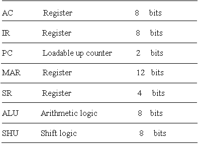
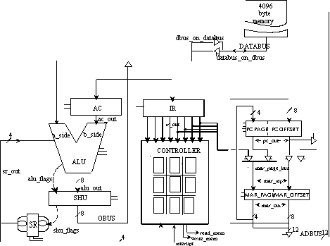
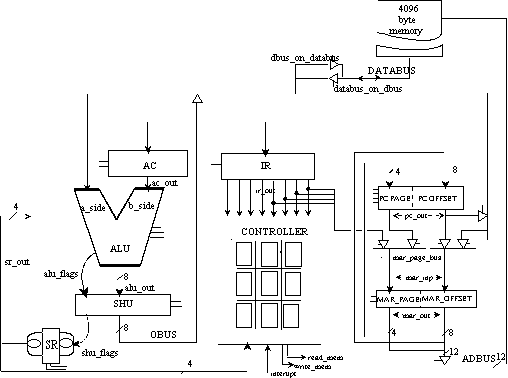
- Machine has 7 components
- Behavioral description helps partitioning the circuit
- Circuit components will be identified
- Bussing specifies interconnection of these components
Data_path.bussing_structure
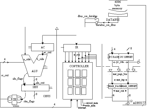
- Bussing provides path for all instructions
- Selection logic used for multi-source buses
Data_path.instruction_execution
lda instruction:
Begin fetch: pc_on_mar_page_bus, pc_on_mar_offset_bus,
load_mar_page, load_mar_offset, increment_pc
mar_on_adbus, read_memory, databus_on_adbus,
alu_a_side_on_alu_output, no_shift, load_ir
Get address: pc_on_mar_page_bus, pc_on_mar_offset_bus,
load_mar_page, load_mar_offset, increment_pc
mar_on_adbus, read_memory, databus_on_dbus,
dbus_on_mar_offset_bus, page_from_ir_on_mar_page_bus
load_mar_page_bus, load_mar_offset_bus
Get operand: mar_on_adbus, read_memory,
load ac databus_on_adbus,
alu_a_side_on_alu_output, no_shift, load_ac
Next fetch : ...
- Steps for execution of lda
Data_path.control_connection
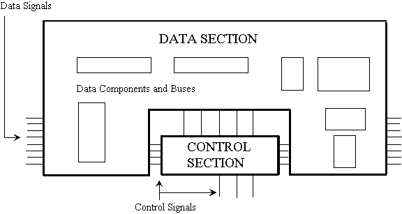
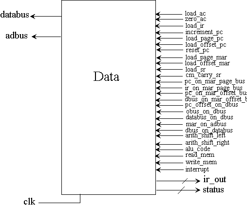
- Signals from control part control data movement
- Same clocking controls both
- All decisions are made in control
- Data part only executes commands
Data_path.control_connection
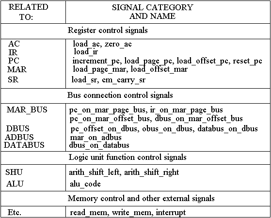
- Lines between data and control
- 23 single bit lines
- alu_code is 3-bit, decoded
Data_path.logic_units
 LIBRARY cmos;
USE cmos.basic_utilities.ALL;
PACKAGE alu_operations IS
CONSTANT a_and_b : qit_vector (2 DOWNTO 0) := "000";
CONSTANT b_compl : qit_vector (2 DOWNTO 0) := "001";
CONSTANT a_input : qit_vector (2 DOWNTO 0) := "100";
CONSTANT a_add_b : qit_vector (2 DOWNTO 0) := "101";
CONSTANT b_input : qit_vector (2 DOWNTO 0) := "110";
CONSTANT a_sub_b : qit_vector (2 DOWNTO 0) := "111";
END alu_operations;
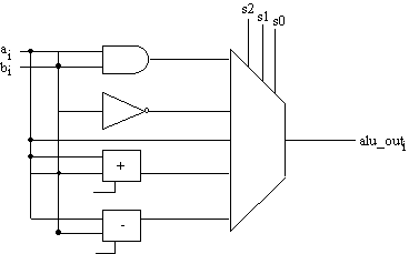
- alu uses decoded select input
- Six operations use three select inputs
- For readability use constants for codes
- For description assume basic_utilities is available
Data_path.logic_units


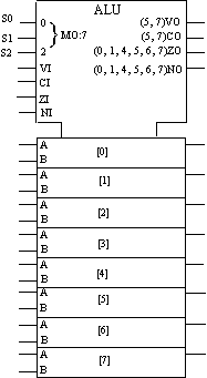
- An 8-bit alu notation
- Operations 5 and 7 effect overflow and carry
- Operations 0,1,4,5,6 and 7 effect all flags
- alu operations are AND, NOT, a_side, Plus, b_side, Minus
Data_path.logic_units
ENTITY arithmetic_logic_unit IS
PORT (a_side, b_side : IN byte; code : IN qit_vector (2 DOWNTO 0);
in_flags : IN nibble; z_out : OUT byte; out_flags : OUT nibble);
END arithmetic_logic_unit;
--
ARCHITECTURE behavioral OF arithmetic_logic_unit IS
BEGIN
coding: PROCESS (a_side, b_side, code)
VARIABLE t : qit_vector (9 DOWNTO 0);
VARIABLE v, c, z, n : qit;
ALIAS n_flag_in : qit IS in_flags(0); ALIAS z_flag_in : qit IS in_flags(1);
ALIAS c_flag_in : qit IS in_flags(2); ALIAS v_flag_in : qit IS in_flags(3);
BEGIN
CASE code IS
WHEN a_add_b => t := add_cv (b_side, a_side, c_flag_in);
c := t(8); v := t(9); -- other flags are set at the end
WHEN a_sub_b => t := sub_cv (b_side, a_side, c_flag_in);
c := t(8); v := t(9);
WHEN a_and_b => t (7 DOWNTO 0) := a_side AND b_side;
c := c_flag_in; v := v_flag_in;
WHEN a_input => t (7 DOWNTO 0) := a_side;
c := c_flag_in; v := v_flag_in;
WHEN b_input => t (7 DOWNTO 0) := b_side;
c := c_flag_in; v := v_flag_in;
WHEN b_compl => t (7 DOWNTO 0) := NOT b_side;
c := c_flag_in; v := v_flag_in;
WHEN OTHERS => NULL;
END CASE;
n := t(7); z := set_if_zero (t); z_out <= t (7 DOWNTO 0);
out_flags <= v & c & z & n;
END PROCESS coding;
END behavioral;
- A behavioral process describes combinational logic
- Use add_cv to produce c and v in bits 8 and 9
- z and n flags are set for all operations
Data_path.logic_units


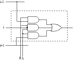
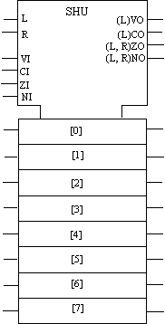
- Shift right or left
- z and n flags are effected by both operations
- Left shift can cause overflow or carry
Data_path.logic_units
- ENTITY shifter_unit IS
- PORT (alu_side : IN byte; arith_shift_left, arith_shift_right : IN qit;
- in_flags : IN nibble; obus_side : OUT byte; out_flags : OUT nibble);
- END shifter_unit;
- --
- ARCHITECTURE behavioral OF shifter_unit IS
- BEGIN
- coding: PROCESS (alu_side, arith_shift_left, arith_shift_right)
- VARIABLE t : qit_vector (7 DOWNTO 0);
- VARIABLE v, c, z, n : qit;
- ALIAS n_flag_in : qit IS in_flags(0); ALIAS z_flag_in : qit IS in_flags(1);
- ALIAS c_flag_in : qit IS in_flags(2); ALIAS v_flag_in : qit IS in_flags(3);
- BEGIN
- IF arith_shift_right = '0' AND arith_shift_left = '0' THEN
- t := alu_side (7 DOWNTO 0);
- n := n_flag_in; z := z_flag_in;
- c := c_flag_in; v := v_flag_in;
- ELSIF arith_shift_left = '1' THEN
- t := alu_side (6 DOWNTO 0) & '0';
- n := t (7); z := set_if_zero (t);
- c := alu_side (7); v := alu_side (6) XOR alu_side (7);
- ELSIF arith_shift_right = '1' THEN
- t := alu_side (7) & alu_side (7 DOWNTO 1);
- n := t (7); z := set_if_zero (t);
- c := c_flag_in; v := v_flag_in;
- END IF;
- obus_side <= t; out_flags <= v & c & z & n;
- END PROCESS coding;
- END behavioral;
- Behavioral description of a combinational logic
- No shift when right and left are 0
- Left shift uses '0' fill
- Right shift extends sign
Data_path.registers


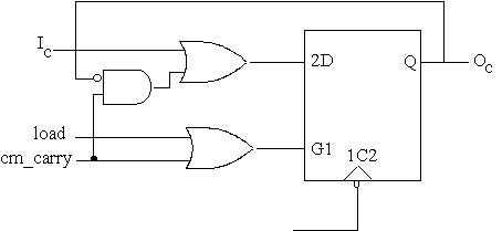
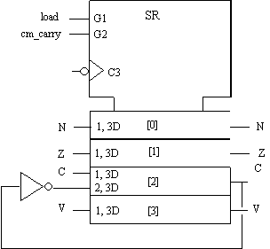
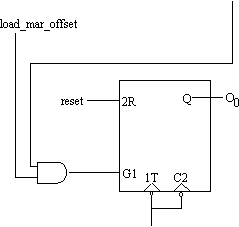
- Status register has four bits
- Load data if load is 1
- Falling edge clock
- load and cm_carry come from control unit
Data_path.registers
- ENTITY status_register_unit IS
- PORT (in_flags : IN nibble; out_status : OUT nibble;
- load, cm_carry, ck : IN qit );
- END status_register_unit;
- --
- ARCHITECTURE behavioral OF status_register_unit IS
- BEGIN
- PROCESS (ck)
- VARIABLE internal_state : nibble := "0000";
- ALIAS internal_z : qit IS internal_state (1);
- ALIAS internal_c : qit IS internal_state (2);
- BEGIN
- IF (ck = '0') THEN
- IF (load = '1') THEN
- internal_state := in_flags;
- ELSIF (cm_carry = '1') THEN
- internal_c := NOT internal_c;
- END IF;
- out_status <= internal_state;
- END IF;
- END PROCESS;
- END behavioral;
- Process is sensitive to clock
- On falling edge, clock for load or cm_carry
- Internal state holds register contents
Data_path.registers


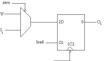
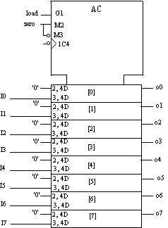
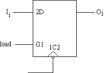
- Accumulator loads 0 or data
- Sensitive to falling edge of clock
- load and zero come from control unit
Data_path.registers
- ENTITY accumulator_unit IS
- PORT (i8 : IN byte; o8 : OUT byte; load, zero, ck : IN qit);
- END accumulator_unit;
- --
- ARCHITECTURE dataflow OF accumulator_unit IS
- BEGIN
- enable : BLOCK (load = '1')
- BEGIN
- clocking : BLOCK ( (ck = '0' AND NOT ck'STABLE) AND GUARD )
- BEGIN
- o8 <= GUARDED "00000000" WHEN zero = '1' ELSE i8;
- END BLOCK clocking;
- END BLOCK enable;
- END dataflow;
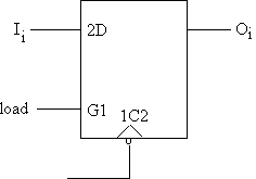
- acVHDL description corresponds to its symbol
- A guarded block statement describes ac
- When load is '1', load on falling edge
Data_path.registers


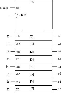
- IR loads on falling edge of clock
- Load input comes from control unit
- IR is a simple 8-bit register
Data_path.registers
- ENTITY instruction_register_unit IS
- PORT (i8 : IN byte; o8 : OUT byte; load, ck : IN qit);
- END instruction_register_unit;
- --
- ARCHITECTURE dataflow OF instruction_register_unit IS
- BEGIN
- enable : BLOCK (load = '1')
- BEGIN
- clocking : BLOCK ( (ck = '0' AND NOT ck'STABLE) AND GUARD )
- BEGIN
- o8 <= GUARDED i8;
- END BLOCK clocking;
- END BLOCK enable;
- END dataflow;
- IR description uses a guarded block
- load and clock edge form guard conditions
Data_path.registers


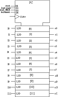
- pc is a 12-bit up counter
- Reset input reset pc to zero
- Separate loads for page and offset
- reset, load_page, load_offset and increment come from control
Data_path.registers
- ENTITY program_counter_unit IS
- PORT (i12 : IN twelve; o12 : OUT twelve;
- increment, load_page, load_offset, reset, ck : IN qit);
- END program_counter_unit;
- --
- ARCHITECTURE behavioral OF program_counter_unit IS
- BEGIN
- PROCESS (ck)
- VARIABLE internal_state : twelve := zero_12;
- BEGIN
- IF (ck = '0' ) THEN
- IF reset = '1' THEN
- internal_state := zero_12;
- ELSIF increment = '1' THEN
- internal_state := inc (internal_state);
- ELSE
- IF load_page = '1' THEN
- internal_state (11 DOWNTO 8) := i12 (11 DOWNTO 8);
- END IF;
- IF load_offset = '1' THEN
- internal_state (7 DOWNTO 0) := i12 (7 DOWNTO 0);
- END IF;
- END IF;
- o12 <= internal_state;
- END IF;
- END PROCESS;
- END behavioral;
- pc description uses a process statement
- On falling edge of clock control inputs are checked
- Internal state holds count value
Data_path.registers


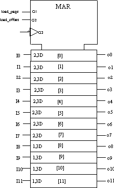
- mar is a simple register
- A 4-bit page part and an 8-bit offset part
- Load inputs come from control part
Data_path.registers
- ENTITY memory_address_register_unit IS
- PORT (i12 : IN twelve; o12 : OUT twelve;
- load_page, load_offset, ck : IN qit);
- END memory_address_register_unit;
- --
- ARCHITECTURE behavioral OF memory_address_register_unit IS
- BEGIN
- PROCESS (ck)
- VARIABLE internal_state : twelve := zero_12;
- BEGIN
- IF (ck = '0' ) THEN
- IF load_page = '1' THEN
- internal_state (11 DOWNTO 8) := i12 (11 DOWNTO 8);
- END IF;
- IF load_offset = '1' THEN
- internal_state (7 DOWNTO 0) := i12 (7 DOWNTO 0);
- END IF;
- o12 <= internal_state;
- END IF;
- END PROCESS;
- END behavioral;
- mar description uses a process statement
- On falling edge of clock loading is done
- Possible to simultaneously load page and offset
- Internal state holds mar contents
Data_path.data_unit

- Control signals from control unit
- ir_out is used by control unit
- status is used by control unit
Data_path.data_unit
- ENTITY par_data_path IS
- PORT (databus : INOUT wired_byte BUS := "ZZZZZZZZ"; adbus : OUT twelve;
- clk : IN qit;
- -- register controls:
- load_ac, zero_ac,
- load_ir,
- increment_pc, load_page_pc, load_offset_pc, reset_pc,
- load_page_mar, load_offset_mar,
- load_sr, cm_carry_sr,
- -- bus connections:
- pc_on_mar_page_bus, ir_on_mar_page_bus,
- pc_on_mar_offset_bus, dbus_on_mar_offset_bus,
- pc_offset_on_dbus, obus_on_dbus, databus_on_dbus,
- mar_on_adbus,
- dbus_on_databus,
- -- logic unit function control inputs:
- arith_shift_left, arith_shift_right : IN qit;
- alu_code : IN qit_vector (2 DOWNTO 0);
- -- outputs to the controller:
- ir_lines : OUT byte; status : OUT nibble
- );
- END par_data_path;
- databus is a three-state resolved bus
- Input control signals are of type qit
- Can drive databus by multiple sources
Data_path.data_unit
- ARCHITECTURE structural OF par_data_path IS
- --
- COMPONENT ac
- PORT (i8: IN byte; o8: OUT byte; load, zero, ck: IN qit);
- END COMPONENT;
- FOR r1: ac USE ENTITY WORK.accumulator_unit (dataflow);
- --
- COMPONENT ir
- PORT (i8: IN byte; o8: OUT byte; load, ck: IN qit);
- END COMPONENT;
- FOR r2: ir USE ENTITY WORK.instruction_register_unit (dataflow);
- --
- COMPONENT pc
- PORT (i12 : IN twelve; o12 : OUT twelve;
- increment, load_page, load_offset, reset, ck : IN qit);
- END COMPONENT;
- FOR r3: pc USE ENTITY WORK.program_counter_unit (behavioral);
- --
- COMPONENT mar
- PORT (i12 : IN twelve; o12 : OUT twelve;
- load_page, load_offset, ck : IN qit);
- END COMPONENT;
- FOR r4: mar USE ENTITY WORK.memory_address_register_unit (behavioral);
- --
- COMPONENT sr
- PORT (in_flags : IN nibble; out_status : OUT nibble;
- load, cm_carry, ck : IN qit );
- END COMPONENT;
- FOR r5 : sr USE ENTITY WORK.status_register_unit (behavioral);
COMPONENT alu PORT (a_side, b_side : IN byte; code : IN qit_vector; in_flags : IN nibble; z_out : OUT byte; out_flags : OUT nibble); END COMPONENT; FOR l1 : alu USE ENTITY WORK.arithmetic_logic_unit (behavioral); -- COMPONENT shu PORT (alu_side : IN byte; arith_shift_left, arith_shift_right : IN qit; in_flags : IN nibble; obus_side : OUT byte; out_flags : OUT nibble); END COMPONENT; FOR l2 : shu USE ENTITY WORK.shifter_unit (behavioral);
- All components are wired together in data unit
- Declare and bind the seven components
Data_path.bus_resolution
- SIGNAL ac_out, ir_out, alu_out, obus : byte;
- SIGNAL alu_a_inp : byte;
- SIGNAL pc_out, mar_out : twelve;
- SIGNAL dbus : wired_byte BUS;
- SIGNAL alu_flags, shu_flags, sr_out : nibble;
- SIGNAL mar_bus : wired_twelve BUS;
- SIGNAL mar_inp : twelve;

- Declare signals for wiring inputs to outputs
- Declare resolved signals for multiple drivers
Data_path.bus_resolution
FUNCTION wire (a, b : qit) RETURN qit IS
CONSTANT qit_and_table : qit_2d := (
('0','X','0','X'),
('X','1','1','X'),
('0','1','Z','X'),
('X','X','X','X'));
BEGIN
RETURN qit_and_table (a, b);
END wire;
FUNCTION wiring ( drivers : qit_vector) RETURN qit IS
VARIABLE accumulate : qit := 'Z';
BEGIN
FOR i IN drivers'RANGE LOOP
accumulate := wire (accumulate, drivers(i));
END LOOP;
RETURN accumulate;
END wiring;
FUNCTION wiring ( drivers : qit_vector) RETURN qit;
SUBTYPE wired_qit IS wiring qit;
TYPE wired_qit_vector IS ARRAY (NATURAL RANGE <>) OF wired_qit;
- Wiring resolution function
- Each bit of the bus is resolved
- Implements hardware three-state wiring
Data_path.component_wiring
ARCHITECTURE
...
BEGIN
Bus connections
Write destinations of each bus
Register connections
Instantiate register, wire to its destinations
Wire registers and logic units
Instantiate logic with register outputs
END Structural
- Data wiring has three parts
- Will describe each part separately
Data_path.component_wiring
- BEGIN
- -- bus connections --
- dbus1: alu_a_inp <= qit_vector (dbus);
- dbus2: BLOCK (dbus_on_mar_offset_bus = '1')
- BEGIN mar_bus (7 DOWNTO 0) <= GUARDED dbus;END BLOCK dbus2;
- dbus3: BLOCK (dbus_on_databus = '1')
- BEGIN databus <= GUARDED dbus; END BLOCK dbus3;
- --
- obus1: BLOCK (obus_on_dbus = '1')
- BEGIN dbus <= GUARDED wired_qit_vector (obus); END BLOCK obus1;
- --
- databus1: BLOCK (databus_on_dbus = '1')
- BEGIN dbus <= GUARDED databus; END BLOCK databus1;
- --
- databus1: BLOCK (databus_on_dbus = '1')
- BEGIN dbus <= GUARDED databus; END BLOCK databus1;
- --
- mar_bus1: mar_inp <= qit_vector (mar_bus);

- dbus is source of alu_a_inp, mar_bus, and databus
- dbus connects directly to alu_a_input, use type conversion
- dbus connects to mar_bus & databus through three-state gates
- Use Block statements for three-state bus connections
- Guard expressions come from control
Data_path.component_wiring
- -- register connections --
- r1: ac PORT MAP (obus, ac_out, load_ac, zero_ac, clk);
- --
- r2: ir PORT MAP (obus, ir_out, load_ir, clk);
- ir1: ir_lines <= ir_out;
- ir2: BLOCK (ir_on_mar_page_bus = '1') BEGIN
- mar_bus (11 DOWNTO 8) <= GUARDED wired_qit_vector (ir_out (3 DOWNTO 0));
- END BLOCK ir2;
- r3: pc PORT MAP (mar_out, pc_out, increment_pc, load_page_pc, load_offset_pc, reset_pc, clk);
- pc1: BLOCK (pc_on_mar_page_bus = '1') BEGIN
- mar_bus (11 DOWNTO 8) <= GUARDED wired_qit_vector (pc_out (11 DOWNTO 8));
- END BLOCK pc1;
- pc2: BLOCK (pc_on_mar_offset_bus = '1') BEGIN
- mar_bus (7 DOWNTO 0) <= GUARDED wired_qit_vector (pc_out (7 DOWNTO 0));
- END BLOCK pc2;
- pc3: BLOCK (pc_offset_on_dbus = '1') BEGIN
- dbus <= GUARDED wired_qit_vector (pc_out (7 DOWNTO 0));
- END BLOCK pc3;
- --
- r4: mar PORT MAP (mar_inp, mar_out, load_page_mar, load_offset_mar, clk);
- mar1: BLOCK (mar_on_adbus = '1') BEGIN
- adbus <= GUARDED mar_out;
- END BLOCK mar1;
- --
- r5: sr PORT MAP (shu_flags, sr_out, load_sr, cm_carry_sr, clk); status <= sr_out;
- END structural;

- Register instantiation
- Blocks are used for register outputs to buses
Data_path.component_wiring
- -- connection of logical and register structures --
- --
- l1: alu PORT MAP (alu_a_inp, ac_out, alu_code, sr_out, alu_out, alu_flags);
- l2: shu PORT MAP (alu_out, arith_shift_left, arith_shift_right, alu_flags, obus, shu_flags);

- alu and shu connections
- shu output is connected to obus
- obus is wire-bussed to dbus
Data_path.conclusion
1. Outline: Introduction, Organization, Outline
2. Review: Levels of abstraction, Entity and Architecture, Signal assignments, Guarded signal assignments, Three state bussing, Process statements, Combinational processes, Sequential processes, Multiplexing, Package
3. MSI Based Design: Use MSI parts of Part 2, Sequential multiplication, Designing the multiplier, Control and data parts, Testing the multiplier
4. General CPU Description: Will present a high level VHDL description of a small CPU. The CPU, Memory organization, Instructions, Addressing, Utilities for VHDL description, Interface, Behavioral description, Coding individual instructions
6. Manual Controller Design: Will present VHDL description for manual design of controller. Controller hardware, VHDL style, Signals and resolutions, State descriptions, Complete CPU, Testing CPU
7. Synthesis: Main concepts, Structural synthesis, Combinational circuits, Functional registers, State machines
8. Behavioral_Synthesis: Will present a high level synthesizable CPU description. Synthesis style, Necessary Package, Interface, General Layout, Registers, Clocking, Sequencing, Simulation and Synthesis
9. Dataflow_Synthesis: Will partition the CPU and synthesize each part separately. Synthesis style, Controller, Data components, Data path, Synthesized example, Conclusions
to the top of the document


 LIBRARY cmos;
