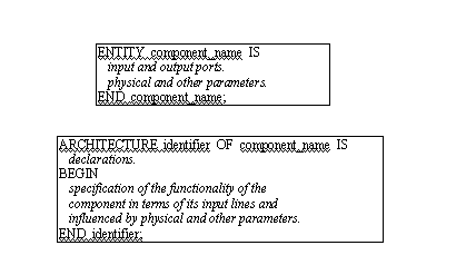

FIGURE 3.1
Interface and architectural specifications.
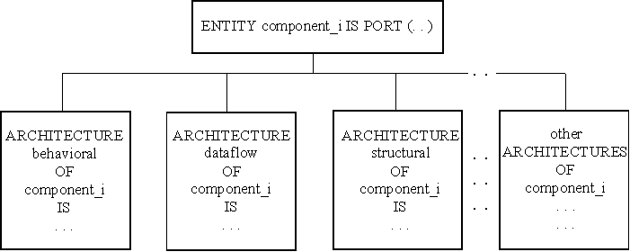
FIGURE 3.2
Multiple architectural specifications.
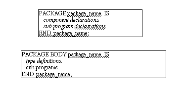
FIGURE 3.3
Packages.
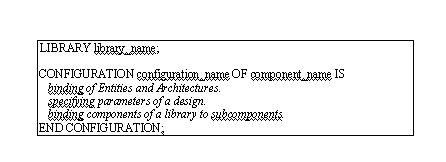
FIGURE 3.4
Design binding.
Partition (system)
IF HardwareMappingOf (system) IS done THEN
SaveHardwareOf (system)
ELSE
FOR EVERY Functionally-Distinct part_i OF system
Partition (part_i);
END FOR;
END IF;
END Partition;
FIGURE 3.5
Recursive partition procedure.
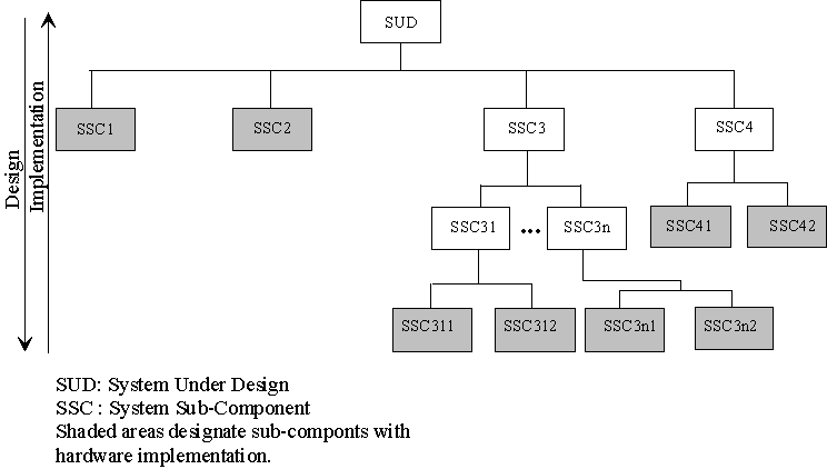
FIGURE 3.6
Top-down design, bottom-up implementation.
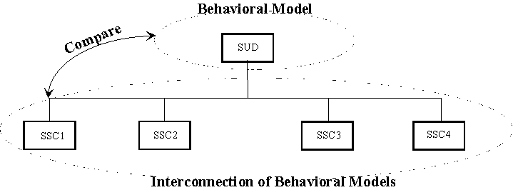
FIGURE 3.7
Verifying the first level of partitioning.
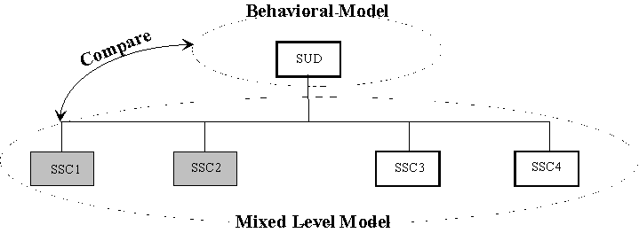
FIGURE 3.8
Verifying hardware implementation of SSC1 and SSC2.
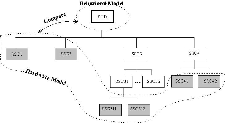
FIGURE 3.9
Verifying the final design.
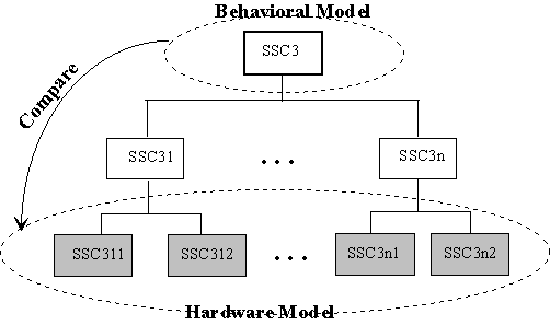
FIGURE 3.10
Verifying hardware implementation of SSC3.
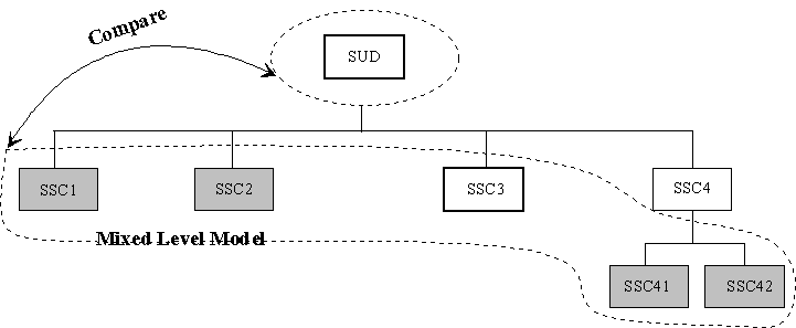
FIGURE 3.11
Verifying the final design, an alternative to the setup of Figure 3.9.

FIGURE 3.12
Serial adder.
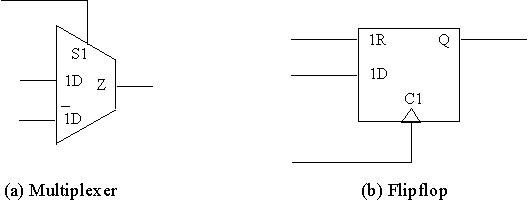
FIGURE 3.13
Available library elements.
FIGURE 3.14
VHDL model of the multiplexer library element.
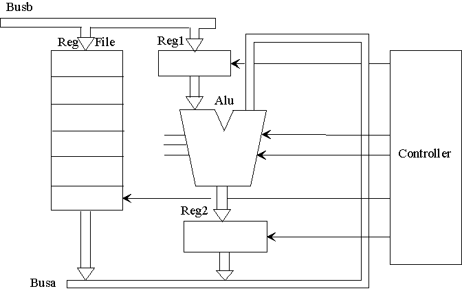
FIGURE 3.15
Dataflow descriptions.
FIGURE 3.16
VHDL model of the flip-flop library element.
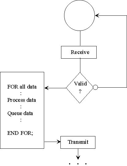
FIGURE 3.17
Behavioral descriptions.
FIGURE 3.18
Divide by 8, counter.
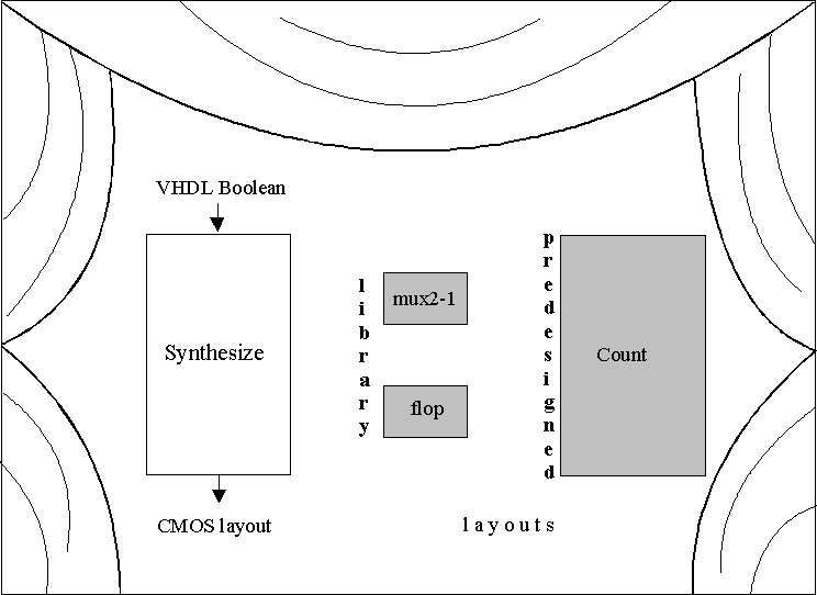
FIGURE 3.19
Design stage setting.
FIGURE 3.20
Serial adder behavioral description.
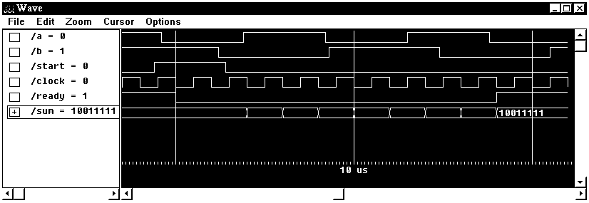
FIGURE 3.21
VHDL simulation results.
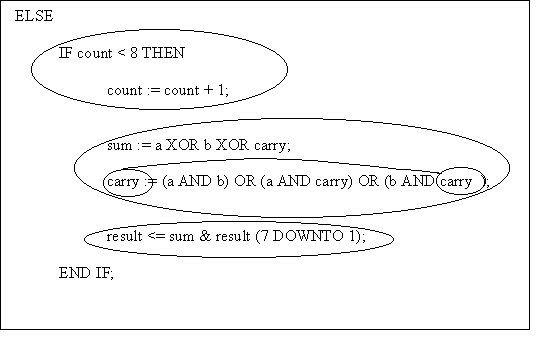
FIGURE 3.22
Partial code of serail_adder.
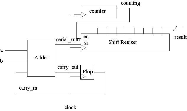
FIGURE 3.23
General layout of serial_adder.

FIGURE 3.24
First level of partitioning.
FIGURE 3.25
Full_adder description.
FIGURE 3.26
Shifter VHDL description.

FIGURE 3.27
Completed parts of first partitioning.
FIGURE 3.28
Structural description of serial_adder.
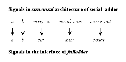
FIGURE 3.29
Signal mapping for fulladder instantiation.
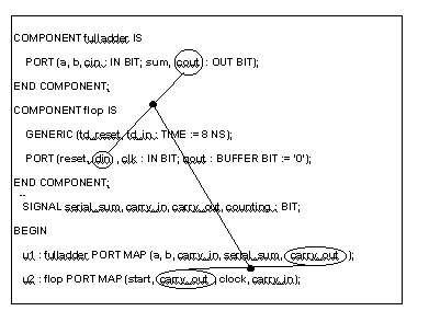
FIGURE 3.30
Interconnecting ports.

FIGURE 3.31
Partitioning shifter.
FIGURE 3.32
Behavioral model of der_flop.
FIGURE 3.33
Structural description of shifter.
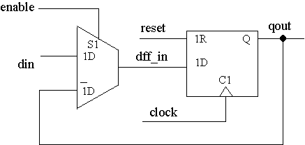
FIGURE 3.34
Hardware realization of der_flop.

FIGURE 3.35
Partitioning der_flop.
FIGURE 3.36
Structural description of der_flop.
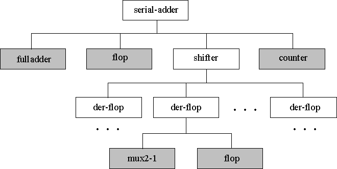
FIGURE 3.37
Complete design of seraial_adder.
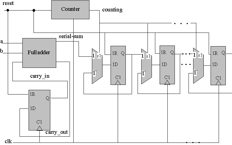
FIGURE 3.38
Final Design.
FIGURE 3.39
Synthesizable serial adder.
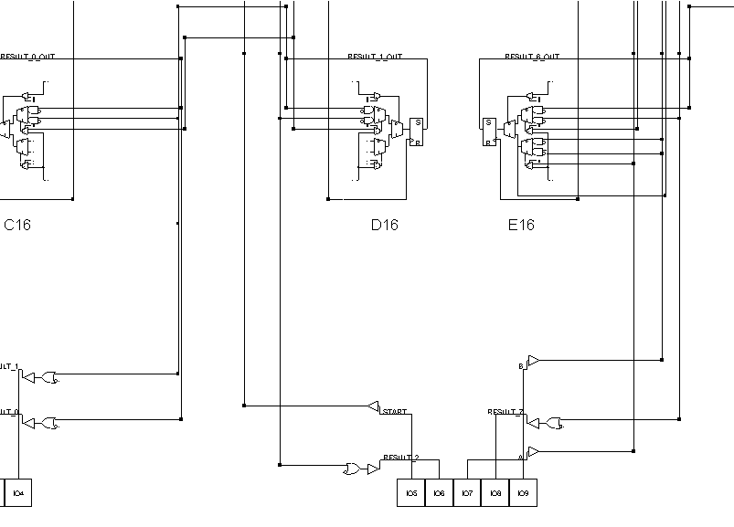
FIGURE 3.40
FPGA layout of serial_adder.
TYPE byte IS ARRAY ( 7 DOWNTO 0 ) OF BIT;
...
PROCEDURE byte_to_integer (ib : IN byte; oi : OUT INTEGER) IS
VARIABLE result : INTEGER := 0;
BEGIN
FOR i IN 0 TO 7 LOOP
IF ib(i) = '1' THEN
result := result + 2**i;
END IF;
END LOOP;
oi := result;
END byte_to_integer;
FIGURE 3.41
Type conversion procedure : converting bytes to integers.
FIGURE 3.42
The fadd (full adder) function.
FIGURE 3.43
fulladder using fadd.
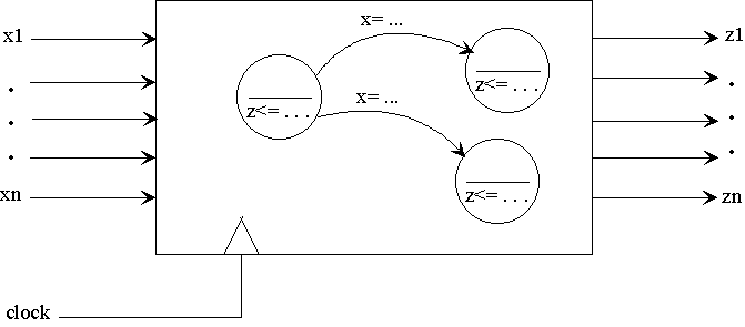
FIGURE 3.44
General outline of a controller.
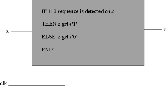
FIGURE 3.45
Moore machine description.
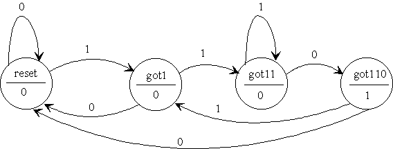
FIGURE 3.46
Sequence detector state machine.
FIGURE 3.47
VHDL Description of 110 detector.
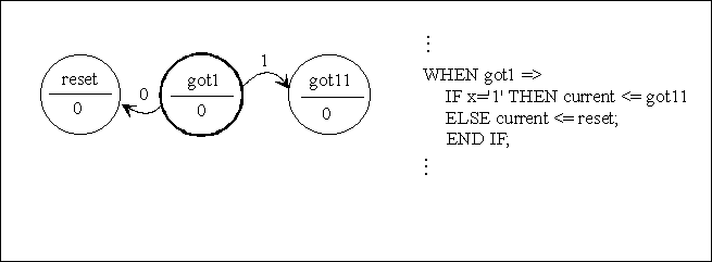
FIGURE 3.48
State transition and corresponding VHDL code.
|
Operators |
Operand Type |
Result Type |
|
|
LOGICAL |
AND OR NAND NOR XOR XNOR |
BIT or BOOLEAN |
BIT or BOOLEAN |
|
RELATIONAL |
= /= < <= > >= |
All Types |
BOOLEAN |
|
SHIFT |
SLL SRL SLA SRA ROL ROR |
Left: BIT or BOOLEAN Vector Right: INTEGER |
BOOLEAN |
|
ADDING |
+ - & |
Numeric Array or Array Element |
Same Type |
|
SIGN |
+ - |
Numeric |
Same Type |
|
MULTIPLYING |
* / |
INTEGER, REAL |
Same Type |
|
MOD REM |
INTEGER |
Same Type |
|
|
MISCELLENEOUS |
ABS |
Numeric |
Same Type |
|
** |
Left: Numeric Right: Integer |
Same as Left |
FIGURE 3.49
VHDL operators.
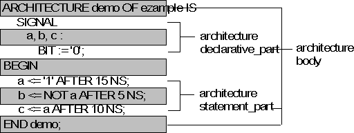
FIGURE 3.50
Syntax details of the architecture body of the demo architecture of example entity.