The WISHBONE System-on-Chip (SoC) architecture is a portable interface for use with semiconductor IP cores. It is intended to be used an an internal bus for SoC applications. Its purpose is to foster design reuse by alleviating System-on-Chip integration problems. This is accomplished by creating a common interface between IP cores. This improves the portability and reliability of the system, and results in faster time-to-market for the end user.
Previously, IP cores used non-standard interconnection schemes that made them difficult to integrate. This required the creation of custom glue logic to connect each of the cores together. By adopting a standard interconnection scheme, the cores can be integrated more quickly and easily by the end user.
This WISHBONE specification can be used for soft core, firm core or hard core IP. Since firm and hard cores are generally conceived as soft cores, the specification is written from that standpoint.
The specification does not require the use of specific development tools or target hardware. Furthermore, it is fully compliant with virtually all logic synthesis tools. However, some of the examples presented in the specification do use the VHDL hardware description language. These are presented only as a convenience to the reader, and should be readily understood by users of other hardware description languages (such as Verilog®). Schematic based entry tools can also be used.
WISHBONE is intended as a general purpose interface. As such, it defines a standard set of signals and bus cycles to be used between IP core modules. It does not attempt to regulate the application specific functions of the IP core.
The WISHBONE architects were strongly influenced by three factors. First, there was a need for a good, reliable System-on-Chip integration solution. Second, there was a need for a common interface specification to facilitate structured design methodologies on large project teams. Third, they were impressed by the traditional system integration solutions afforded by microcomputer buses such as PCI bus and VMEbus.
In fact, the WISHBONE architecture is analogous to a microcomputer bus in that that they both: (a) offer flexible integration solutions that can be easily tailored to each application; (b) offer a variety of bus cycles and data path widths to solve various system problems; and (c) allow products to be designed by a variety of suppliers (thereby driving down price while improving performance and quality).
Traditional microcomputer buses are not appropriate use as System-on-Chip (SoC) interconnections. That's because they must drive backplane signal traces and connectors which are both highly inductive and capacitive. In this regard, SoC integration is much simpler and faster. Furthermore, integrated circuit solutions have a rich set of interconnection resources. These do not exist in microcomputer buses because they are limited by IC packaging and mechanical connectors.
The WISHBONE architects have attempted to create a specification that is robust enough to insure complete compatibility between IP cores. However, it has not been over specified so as to unduly constrain the creativity of the core developer or the end user. It is believed that these two goals have been accomplished with the WISHBONE specification.
- Simple, compact, logical IP core hardware interface requires very few logic gates.
- Full set of popular data transfer bus protocols including: single READ / WRITE cycle, BLOCK transfer cycle, RMW (read-modify-write) cycle and an EVENT cycle.
- Data bus widths and operand sizes from 8 to 64-bits (expandable).
- Supports both BIG ENDIAN and LITTLE ENDIAN data ordering.
- Flexible interface supports memory mapped, FIFO memory and crossbar interconnections.
- Handshaking protocol allows each core to throttle data transfer speed.
- Up to one data transfer per clock cycle.
- Supports normal cycle termination, retry termination and error termination of bus cycles.
- Address widths up to 64-bits.
- User-defined tag support. This is useful for discriminating between data transfers, interrupt vectors, cache control operations and other bus transactions.
- MASTER / SLAVE architecture for very flexible system designs.
- Multiprocessing (multi-MASTER) capabilities. This allows for a wide variety of System-on-Chip configurations. Furthermore, it can be used in crossbar switches.
- Arbitration methodology is defined by the end user (priority arbiter, round-robin arbiter, etc.).
- Supports various types of IP core interconnections including: unidirectional bus, bi-directional bus, multiplexer based interconnections, three-state based interconnections and off-chip I/O.
- Synchronous design assures portability, simple design and ease of test.
- Very simple timing specification.
- Documentation requirements allow the end user to quickly evaluate each interface.
- Independent of hardware technology (FPGA, ASIC, bipolar, MOS etc.).
- Independent of delivery method (i.e. soft, firm or hard core).
- Independent of synthesis tool, router and layout tool technology.
WISHBONE is an excellent tool for use with structured design methodologies. Structured design is a popular way to manage complex projects. When structured design practices are used, individual team members build and test small pieces of the design. Each of these pieces are designed to interface to a known specification. When all of the sub-assemblies have been designed and tested, then the full system is integrated and tested.
Structured design is also popular among software engineers. For example, the C, C++ and JAVA programming languages incorporate structured design principles.
Structured design methodologies are also a popular way of managing concurrent engineering. Concurrent engineering is a project management tool where many parts of an engineering task are done at the same time. It's a good way to shorten the time-to-market in complex systems.
WISHBONE supports structured design by providing a common interface for all of the pieces of the system. Each team member designs their part of the system to the WISHBONE standard. These can then be integrated together very easily. Also, at the sub-assembly level, the WISHBONE interface is quite simple and does not add significantly to the overall gate count of the finished device. In some cases it does not add any extra gates at all.
Webster's dictionary defines a WISHBONE as "the forked clavicle in front of the breastbone of most birds." The term 'WISHBONE interconnect' was coined by Wade Peterson of Silicore Corporation. During the initial definition of the bus he was attempting to find a descriptive name for a bi-directional data bus that used either multiplexors or three-state logic. This was solved by forming an interface with separate input and output paths. When these paths are connected to three-state logic it forms a 'Y' shaped configuration that resembles a WISHBONE. The actual name was conceived during a Thanksgiving Day turkey dinner. Thanksgiving Day is a national holiday in the United States, and is observed on the third Thursday in November.
The WISHBONE name is not known to be trademarked in the area
of semiconductor products. The name was placed into the public
domain by the publication of the WISHBONE specification.
The WISHBONE architecture solves a very basic problem in integrated circuit design. That is, how to connect circuit functions together in a way that is simple, flexible and portable. The circuit functions are generally provided as 'IP Cores' (Intellectual Property Cores), which system integrators can obtain as open source, purchase or make themselves.
Under this topology, IP Cores are the functional building blocks in the system. They are available in a wide variety of functions such as microprocessors, serial ports, disk interfaces, network controllers and so forth. Generally, the IP cores are developed independently from each other and are tied together and tested by a third party system integrator. WISHBONE aides the system integrator by standardizing the IP Core interfaces. This makes it much easier to connect the cores, and therefore much easier to create a custom System-on-Chip.
WISHBONE uses a MASTER/SLAVE architecture. That means that functional modules with MASTER interfaces initiate data transactions to participating SLAVE interfaces. As shown in Figure 1, the MASTERs and SLAVEs communicate through an interconnection interface called the INTERCON. The INTERCON is best thought of as a 'cloud' that contains circuits. These circuits allow MASTERs to communicate with SLAVEs.
The term 'cloud' is borrowed from the telecom community. There, telephone systems are modeled as clouds that represent a system of telephone switches and transmission devices. Telephone handsets are connected to the cloud, and are used to make phone calls. The cloud itself represents a network that carries a telephone call from one location to another. The activity going on inside the cloud depends upon where the call is made and where it is going. For example, if a call is made to another office down the hall, then the cloud may represent a local telephone switch located in the same building. However, if the call is made across an ocean, then the cloud may represent a combination of copper, fiber optic and satellite transmission systems. WISHBONE works in a similar way.
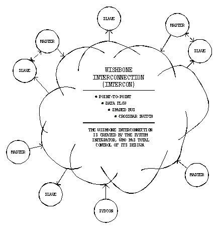
The cloud analogy makes sense because WISHBONE can be thought of in the same way. MASTER and SLAVE interfaces (which are analogous to the telephones) communicate thorough an interconnection (which is analogous to the telephone network 'cloud'). The WISHBONE interconnection network can be changed by the system integrator to suit his or her own needs. In WISHBONE terminology this is called a variable interconnection.
Variable interconnection allows the system integrator to change the way in which the MASTER and SLAVE interfaces communicate with each other. For example, a pair of MASTER and SLAVE interfaces can communicate with point-to-point, data flow, shared bus or crossbar switch topologies.
The variable interconnection scheme is very different from that used in traditional microcomputer buses such as PCI, cPCI, VMEbus and ISA bus. Those systems use printed circuit backplanes with hardwired connectors. The interfaces on those buses can't be changed, which severely limits how microcomputer boards communicate with each other. WISHBONE overcomes this limitation by allowing the system integrator to change the system interconnection.
This is possible because integrated circuit chips have interconnection paths that can be adjusted. These are very flexible, and take the form of logic gates and routing paths. These can be 'programmed' into the chip using a variety of tools. For example, if the interconnection is described with a hardware description language like VHDL or Verilog(R), then the system integrator has the ability to define and adjust the interconnection. Interconnection libraries can also be formed and shared.
The WISHBONE interconnection itself is nothing more than a large, synchronous circuit. It must be designed to logically operate over a nearly infinite frequency range. However, every integrated circuit has physical characteristics that limit the maximum frequency of the circuit. In WISHBONE terminology this is called a variable timing specification. This means that a WISHBONE compatible circuit must theoretically function normally at any speed (i.e. DC to light) , but that it's maximum speed will always be limited by the process technology of the integrated circuit.
At Silicore Corporation we generally define our WISHBONE interconnections using the VHDL hardware description language. These take the form of an ASCII file that contains the VHDL language instructions. This allows us to fully define our interconnections in a way that best fits the application. However, it also allows us to share our interconnections with others, who can adjust them to meet their own needs. It's important to note, though, that there's nothing magic about the interconnection itself. It's just a file, written with off-the-shelf tools, that fully describes the hardware in the interconnection.
The WISHBONE variable interconnection allows the system integrator to change the way that IP cores connect to each other. This is important because there is no, single right way to do every SoC. There are four defined types of WISHBONE interconnection, and include:
- Point-to-point
- Data flow
- Shared bus
- Crossbar switch
A fifth possible type is the off-chip interconnection. However, off-chip implementations generally fit one of the other four basic types. For example, WISHBONE interfaces on two different integrated circuits can be connected using a point-to-point interconnection.
The WISHBONE specification does not dictate how any of these are implemented by the system integrator. That's because the interconnection itself is a type of IP Core interface called the INTERCON. The system integrator can use or modify an off-the-shelf INTERCON, or create their own.
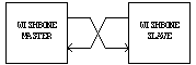
Point-to-point Interconnection
The point-to-point interconnection is the simplest way to connect two WISHBONE IP cores together. As shown in Figure 2, the point-to-point interconnection allows a single MASTER interface to connect to a single SLAVE interface. For example, the MASTER interface could be on a microprocessor IP core, and the SLAVE interface could be on a serial I/O port.
Data Flow Interconnection
The data flow interconnection is used when data is processed in a sequential manner. As shown in Figure 3, each IP core in the data flow architecture has both a MASTER and a SLAVE interface. Data flows from core-to-core. Sometimes this process is called pipelining.
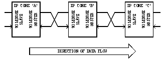
The data flow architecture exploits parallelism, thereby speeding up execution time. For example, if each of the IP cores in the Figure represents a floating point processor, then the system has three times the number crunching potential of a single unit. This assumes, of course, that each IP Core takes an equal amount of time to solve its problem, and that the problem can be solved in a sequential manner. In actual practice this may or may not be true, but it does illustrate how the data flow architecture can provide a high degree of parallelism when solving problems.
Shared Bus Interconnection
The shared bus interconnection is useful for connecting two or more MASTERs with one or more SLAVEs. A block diagram is shown in Figure 4. In this topology a MASTER initiates a bus cycle to a target SLAVE. The target SLAVE then participates in one or more bus cycles with the MASTER.
An arbiter (not shown in the Figure) determines when a MASTER may gain access to the shared bus. The arbiter acts like a 'traffic cop' to determine when and how each MASTER accesses the shared resource. Also, the type of arbiter is completely defined by the system integrator. For example, the shared bus can use a priority or a round robin arbiter. These grant the shared bus on a priority or equal basis, respectively.
The main advantage to this technique is that shared interconnection systems are relatively compact. Generally, it requires fewer logic gates and routing resources than other configurations, especially the crossbar switch. Its main disadvantage is that MASTERs may have to wait before gaining access to the interconnection. This degrades the overall speed at which a MASTER may transfer data.
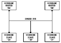
The WISHBONE specification does not dictate how the shared bus is implemented. Later on, we'll see that it can be made either with multiplexer or three-state buses. This gives the system integrator additional flexibility, as some target devices work better with multiplexor logic, and some work better with three-state buses. If you would like to see a diagram of a classic WISHBONE shared bus, then you can download a diagram of one ('ShardBus.pdf', 17 Kb).
The shared bus is typically found in standard buses like PCI and VMEbus. There, a MASTER interface arbitrates for the common shared bus, and then communicates with a SLAVE. The WISHBONE shared bus can be viewed in a similar way. For example, if you rotate the shared bus diagram given above by 90 degrees (i.e. 'ShardBus.pdf' rotated clockwise), then you end up with a diagram that shows how to view WISHBONE like a traditional microcomputer bus. You can download a modified sketch that shows this concept (ShardBusCompare.pdf, 179 Kb). For example, the modified sketch shows how the WISHBONE MASTER and SLAVE interfaces are analogous to connectors on a single microcomputer board. There, the IP Core is like a microcomputer board, and the MASTER and SLAVE interfaces are like the connectors. These are plugged into the WISHBONE INTERCON, which is analogous to a backplane. The WISHBONE INTERCON contains the interconnections, as well as other logic like an arbiter, address comparitor and SYSCON.
Crossbar Switch Interconnection
The crossbar switch interconnection is used when connecting two or more WISHBONE MASTERs together so that each can access two or more SLAVEs. A block diagram is shown in Figure 5. In the crossbar interconnection, a MASTER initiates an addressable bus cycle to a target SLAVE. An arbiter (not shown in the diagram) determines when each MASTER may gain access to the indicated SLAVE. Unlike the shared bus interconnection, the crossbar switch allows more than one MASTER to use the interconnection (as long as two MASTERs don't access the same SLAVE at the same time).
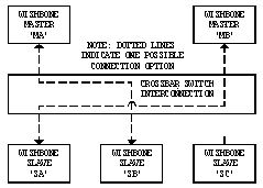
Under this method, each master arbitrates for a 'channel' on the switch. Once this is established, data is transferred between the MASTER and the SLAVE over a private communication link. The Figure shows two possible channels that may appear on the switch. The first connects MASTER 'MA' to SLAVE 'SB'. The second connects MASTER 'MB' to SLAVE 'SA'.
The overall data transfer rate of the crossbar switch is higher than shared bus mechanisms. For example, the figure shows two MASTER/SLAVE pairs interconnected at the same time. If each communication channel supports a data rate of 100 Mbyte/sec, then the two data pairs would operate in parallel at 200 Mbyte/sec. This scheme can be expanded to support extremely high data transfer rates.
If you would like to see a diagram of a classic WISHBONE crossbar switch, then you can download a diagram of one ('CrossBar.pdf', 17 Kb).
One disadvantage of the crossbar switch is that it requires more interconnection logic and routing resources than shared bus systems. As a rule-of-thumb, a crossbar switch with two MASTERs and two SLAVEs takes twice as much interconnection logic as a similar shared bus system (with two MASTERs and two SLAVEs).
The crossbar interconnection is a typical configuration that one might find in microcomputer buses like RACEway, SKY Channel or Myrinet.
MASTER and SLAVE interfaces each have a unique set of signals. Most of these are optional, and may or may not be present on a specific interface. WISHBONE uses a logical interface which means that the IP cores are logically connected with the system integrator's development tools. For example, VHDL soft IP cores would be connected together with descriptions in an entity/architecture pair.
Consider the two interconnected MASTER / SLAVE IP cores shown in Figure 6. These show how the signals interconnect a MASTER and SLAVE interfaces to form a point-to-point interconnection. The end user forms these interconnections with his/her development tools.
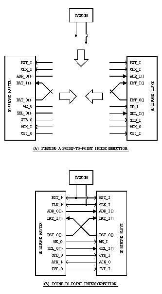
Table 1 presents signal descriptions that can be used by the MASTER interface. The SLAVE has a similar set of signals that are not shown in Table 1. For a complete list of WISHBONE signals, the user is directed to the specification document.
Table 1 - MASTER signals.
|
|
|
|
|
The acknowledge input [ACK_I], when asserted, indicates the termination of a normal bus cycle. Also see the [ERR_I] and [RTY_I] signal descriptions. |
|
|
The address output array [ADR_O(63..0)] is used to pass a binary address, with the most significant address bit at the higher numbered end of the signal array. The lower array boundary is specific to the data port size. The higher array boundary is core-specific. In some cases (such as FIFO interfaces) the array may not be present on the interface. |
|
|
The clock input [CLK_I] coordinates all activities for the internal logic within the WISHBONE interconnect. All WISHBONE output signals are registered at the rising edge of [CLK_I]. All WISHBONE input signals must be stable before the rising edge of [CLK_I]. |
|
|
The cycle output [CYC_O], when asserted, indicates that a valid bus cycle is in progress. The signal is asserted for the duration of all bus cycles. For example, during a BLOCK transfer cycle there can be multiple data transfers. The [CYC_O] signal is asserted during the first data transfer, and remains asserted until the last data transfer. The [CYC_O] signal is useful for interfaces with multi-port interfaces (such as dual port memories). In these cases, the [CYC_O] signal requests use of a common bus from an arbiter. Once the arbiter grants the bus to the MASTER, it is held until [CYC_O] is negated. |
|
|
The data input array [DAT_I(63..0)] is used to pass binary data. The array boundaries are determined by the port size. Also see the [DAT_O(63..0)] and [SEL_O(7..0)] signal descriptions. |
|
|
The data output array [DAT_O(63..0)] is used to pass binary data. The array boundaries are determined by the port size. Also see the [DAT_I(63..0)] and [SEL_O(7..0)] signal descriptions. |
|
|
The error input [ERR_I] indicates an abnormal cycle termination. The source of the error, and the response generated by the MASTER is defined by the IP core supplier in the WISHBONE DATASHEET. Also see the [ACK_I] and [RTY_I] signal descriptions. |
|
|
The reset input [RST_I] forces the WISHBONE interface to restart. Furthermore, all internal self-starting state machines will be forced into an initial state. |
|
|
The retry input [RTY_I] indicates that the indicates that the interface is not ready to accept or send data, and that the cycle should be retried. When and how the cycle is retried is defined by the IP core supplier in the WISHBONE DATASHEET. Also see the [ERR_I] and [RTY_I] signal descriptions. |
|
|
The select output array [SEL_O(7..0)] indicates where valid data is expected on the [DAT_I(63..0)] signal array during READ cycles, and where it is placed on the [DAT_O(63..0)] signal array during WRITE cycles. Also see the [DAT_I(63..0)], [DAT_O(63..0)] and [STB_O] signal descriptions. |
|
|
The strobe output [STB_O] indicates a valid data transfer cycle. It is used to qualify various other signals on the interface such as [SEL_O(7..0)]. The SLAVE must assert either the [ACK_I], [ERR_I] or [RTY_I] signals in response to every assertion of the [STB_O] signal. |
|
|
The tag signals [TAGN_I] and [TAGN_O] are user defined and are used by both MASTER and SLAVE modules. They are used for three purposes: (a) to tag data with information such as parity or time stamps, (b) to identify specialty bus cycles (like interrupts or cache control operations) and (c) to facilitate communication between an IP core and teh bus interconnection. Any number of tags can be defined by the user, where 'N' is the tag number (e.g. [TAG6_I]). The exact meaning of each tag is defined by the IP core provider in the WISHBONE DATASHEET. |
|
|
The write enable output [WE_O] indicates whether the current local bus cycle is a READ or WRITE cycle. The signal is negated during READ cycles, and is asserted during WRITE cycles. |
The WISHBONE specification uses a set of standard signal names for descriptive purposes. However, any signal name can be chosen by the IP core developer as long as it is in accordance with the rules of the native tool in which the IP core was designed. Core integration is simplified if the signal names match those given in the specification, but isn't required. The use of non-standard signal names will not result in any serious integration problems since all hardware description tools allow signals to be renamed.
All signal names used in the specification have the '_I' or '_O' characters attached to them. These indicate if the signals are an input (to the core) or an output (from the core). For example, [ACK_I] is an input to a MASTER and [ACK_O] is an output from a SLAVE. This convention is used to clearly identify the direction of each signal.
Signal arrays are identified by a signal name followed by the array boundaries in parenthesis. For example, [DAT_I(63..0)] is a signal array with upper array boundary number sixty-three, and lower array boundary number zero.
The WISHBONE specification defines four types of bus cycles: the READ / WRITE cycle, the BLOCK transfer cycle, the RMW (read-modify-write) cycle and the EVENT cycle. In this tutorial we'll discuss the general purpose READ / WRITE and BLOCK transfer cycles. The RMW and EVENT cycles are somewhat specialized, and the reader is directed to the WISHBONE specification for more information.
Handshaking Protocol
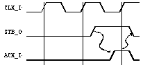
All WISHBONE bus cycles use a handshaking protocol between the MASTER and SLAVE interfaces. As shown in Figure 7, the MASTER asserts [STB_O] when it is ready to transfer data. [STB_O] remains asserted until the SLAVE asserts one of the cycle terminating signals [ACK_I], [ERR_I] or [RTY_I]. At every rising edge of [CLK_I] the terminating signal is sampled. If it is asserted, then [STB_O] is negated. Both sides of the interface can then completely control the rate at which data is transferred. If the SLAVE always operates at the maximum speed of the core, and if the [ERR_I] and [RTY_I] signals are not used, then the [ACK_O] signal may be asserted by the slave immediately after it receives [STB_I]. The interface will function normally under these circumstances.
All of the examples in this tutorial describe the use of [ACK_O] to terminate a local bus cycle. However, the SLAVE can optionally terminate the cycle with an error [ERR_O], or request that the cycle be retried with [RTY_O].
All interfaces include the [ACK_O] terminator signal. Asserting this signal during a bus cycle causes it to terminate normally.
Asserting the optional [ERR_O] signal during a bus cycle will terminate the cycle. It also serves to notify the MASTER that an error occurred during the cycle. This signal is generally used if an error was detected by SLAVE logic circuitry. For example, if the SLAVE has a parity-protected memory, then its [ERR_O] signal can be asserted if a parity fault is detected. The specification does not dictate what the MASTER will do in response to [ERR_I].
Asserting the optional [RTY_O] signal will terminate a bus cycle. It also serves to notify the MASTER that the current cycle should be aborted, and retried at a later time. This signal is generally used for shared memory and bus bridges. In these cases, SLAVE circuitry would assert [RTY_O] if the local resource is busy. The specification does not dictate when or how the MASTER will respond to [RTY_I].
Timing
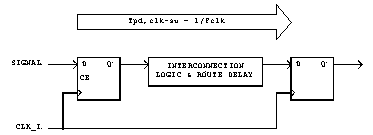
The WISHBONE specification is designed to provide the end user with very simple timing constraints. Although the application specific circuit(s) will vary in this regard, the interface itself is designed to work without the need for detailed timing specifications. In all cases, the only timing information that is needed by the end user is the maximum clock frequency that is passed to a place & route tool. The maximum clock frequency is dictated by the time delay between a positive clock edge on [CLK_I] to the setup to a stage further down the logical signal path. This delay is shown graphically in Figure 8, and is defined as Tpd,clk-su. Most place and route tools can be easily configured to enforce this timing. Generally, it only requires a single timing specification for Tpd,clk-su.
The clock input [CLK_I] to each IP core coordinates all activities for the internal logic within the WISHBONE interface. All WISHBONE output signals are registered at the rising edge of [CLK_I]. All WISHBONE input signals must be stable before the rising edge of [CLK_I].
The WISHBONE interface must use synchronous, RTL design methodologies that, given nearly infinitely fast gate delays, will operate over a nearly infinite range of clock frequencies on [CLK_I]. Realistically, the WISHBONE interface will never be expected to operate over a nearly infinite frequency range. However this requirement eliminates the need for non-portable timing constraints (that may work only on certain target devices). Furthermore, these constraints allow a smooth upgrade path to faster chip technologies as they become available in the future.
The WISHBONE interface logic assumes that a low-skew clock distribution scheme is used on the target device, and that the clock-skew is low enough to permit reliable operation over the environmental conditions.
Single READ / WRITE Cycles
The single READ / WRITE cycles are the basic modes of data transfer. The timing diagram for a single READ cycle is shown in Figure 9. There, the MASTER begins the cycle at the rising edge of clock edge 0. At that time it places an address onto address bus [ADR_O()], negates the [WE_O] line to indicate a READ cycle, drives the data select line(s) [SEL_O()] high or low depending upon the location that is being read, and asserts [STB_O] and [CYC_O] to indicate the start of a new bus cycle.
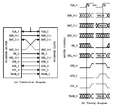
The interconnection logic decodes the address and responds by placing asserting [STB_I] to the SLAVE. The SLAVE then places data on its data output bus [DAT_O()]. The SLAVE then terminates the cycle by asserting [ACK_O]. This informs the MASTER that it should latch the data on the next rising edge of [CLK_I]. After latching the data, the MASTER terminates the cycle by negating [STB_O].
The WRITE cycle is similar to the READ cycle. However, in this case the MASTER negates [WE_O] and presents valid data out on [DAT_O()] at the beginning of the cycle. In response, the SLAVE asserts [ACK_O] when it is ready to latch the data at the next rising edge of [CLK_I].
Each WISHBONE MASTER or SLAVE can drive one or more optional [TAGN_X] signals. These are user-defined tags that accompany each data transfer, and allows various types of data to be discriminated from each other. This means that each bus cycle can be identified as to it's purpose. For example, in microprocessor based systems it is often necessary to discriminate between data transfer, interrupt acknowledge and caching operations.
The [CYC_O] signal is mainly used for multi MASTER systems. This signal is asserted for the duration of all bus cycles, and is intended for use by a bus arbiter.
This example also illustrates how the SLAVE can throttle the data transfer speed by holding off the assertion of [ACK_O]. Similarly, the MASTER can throttle the data transfer speed by holding off the assertion of [STB_O] at the beginning of the cycle.
BLOCK Cycle
The BLOCK transfer cycles perform multiple data transfers. They are very similar to single READ and WRITE cycles, but have a few special modifications to support multiple transfers.
During BLOCK cycles, the interface basically performs SINGLE READ/WRITE cycles as described above. However, the BLOCK cycles are modified somewhat so that these individual cycles are combined together to form a single BLOCK cycle. This function is most useful when multiple MASTERs are used on the interconnect. For example, the system arbiter can determine when one MASTER is done with the interconnection bus so that another MASTER can gain access to the SLAVEs.
As shown in Figure 10, the [CYC_O] signal is asserted for the duration of a BLOCK cycle. This signal can be used to request permission to access a SLAVE from a local arbiter, and hold the access until the end of the current cycle. During each of the data transfers (within the block transfer), the normal handshaking protocol between [STB_O] and [ACK_I] is maintained.
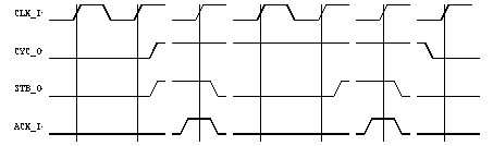
It should be noted that the [CYC_O] signal does not necessarily rise and fall at the same time as [STB_O]. It may be asserted at the same time as [STB_O], or one or more [CLK_I] edges before [STB_O]. Similarly, it may be negated at the same time as [STB_O], or an indeterminate number of clock cycles afterwards.
A sample BLOCK WRITE cycle is shown in Figure 11. This cycle also shows how both the MASTER and the SLAVE can throttle the bus transaction rate.

Data Organization
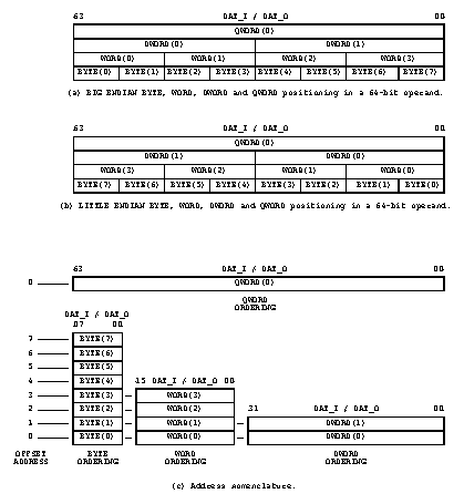
Data organization refers to the ordering of data during transfers. There are two general types of ordering which are called BIG ENDIAN and LITTLE ENDIAN. BIG ENDIAN refers to data ordering where the most significant portion of an operand is stored at the lower address. LITTLE ENDIAN refers to data ordering where the most significant portion of an operand is stored at the higher address. The WISHBONE architecture supports both methods of data ordering.
A BYTE(N), WORD(N), DWORD(N) and QWORD(N) nomenclature is used to define data ordering. These terms are defined in Table 2. The table also defines the granularity of the interface. Granularity is the minimum unit of data transfer that is supported by the interface. For example, the smallest operand that can be passed through a port with 16-bit granularity is a 16-bit WORD. In this case, an 8-bit operand cannot be transferred.
Table 2 - Data transfer nomenclature.
|
|
|
|
|
|
|
An 8-bit BYTE transfer at address 'N'. |
|
|
|
A 16-bit WORD transfer at address 'N'. |
|
|
|
A 32-bit DWORD transfer at address 'N'. |
|
|
|
A 64-bit QWORD transfer at address 'N'. |
Figure 12 shows the operand locations for input and output data ports. The WISHBONE architecture is extremely flexible in terms of data organization. Virtually any size of data operand between eight and sixty-four bits can be moved through virtually any data port size. Furthermore, the BIG ENDIAN and LITTLE ENDIAN ordering can be used.
Fundamentally, there is no limit to the width of the WISHBONE data interface. It can theoretically be extended beyond 64-bits. However, the standard only defines the data port sizes up to 64-bits.
Logic Overhead Required for the Interface
In most cases the WISHBONE interface is very efficient in terms of logic gate count. This is because WISHBONE is designed to work in conjunction with standard, synchronous logic primitives that are available on most FPGA and ASIC devices. In many cases, the WISHBONE interface does not require any extra logic gates whatsoever.
For example, Figure 13 shows a simple 8-bit parallel output port. The entire interface is implemented with a standard 8-bit 'D-type' flip-flop register (with synchronous reset) and a single AND gate. During write cycles, data is presented at the data input bus [DAT_I(7..0)], and is latched at the rising edge of [CLK_I] when [STB_I] and [WE_I] are both asserted.
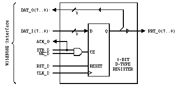
Figure 14 shows a simple 8-bit WISHBONE memory that is also highly efficient. The 16 x 8-bit memory is formed from two 16 x 4-bit synchronous memory primitives (available on most FPGA and ASIC devices). Besides the memory elements, the entire interface is implemented with a standard AND gate. During write cycles, data is presented at the data input bus [DAT_I(7..0)], and is latched at the rising edge of [CLK_I] when [STB_I] and [WE_I] are both asserted. During read cycles, the memory output data (DO) is made available at the data output port [DAT_O(7..0)].
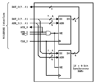
It can be seen from these two examples that the WISHBONE interface is very efficient in terms of logic gate count. It works in conjunction with standard logic primitives, and adds very few (if any) additional gates to the interface.
Application Interface
The WISHBONE specification defines four ways to integrate IP cores. These include:
- Single MASTER / Single SLAVE interconnection
- Single MASTER / Multiple SLAVE interconnection
- Multiple MASTER interconnection
- Crossbar interconnection.
Furthermore, three-state interconnections, as well as BIG ENDIAN to LITTLE ENDIAN conversions are discussed in the specification. For more information the user is directed to the WISHBONE specification.
Documentation Standards
Documentation must be provided for each IP core with a WISHBONE interconnect. This helps the end user understand the operation of the core, and how to connect it to other cores. The documentation takes the form of a WISHBONE DATASHEET. This can be included in a technical reference manual for the IP core.
The WISHBONE DATASHEET contains such information as address and data port sizes, data organization, types of bus cycles performed and so forth.
The speed of the WISHBONE systems varies widely, and ultimately depends upon the speed of the target FPGA or ASIC device. Table 3 shows some benchmarks for the point-to-point and shared bus interconnections. These were synthesized and routed for Xilinx Spartan 2 and Virtex 2 FPGAs. You can also examine, synthesize and run these same benchmarks on your own tools and target device. Complete instructions can be found in Appendix A of the WISHBONE specification. VHDL source code and test benches for the same benchmarks can be found in the WISHBONE Public Domain Library for VHDL. The benchmark code (that comes with the library) is also a good way to see how real WISHBONE interfaces and interconnections work.
|
|
||
|
|
|
(MAX) |
|
|
Xilinx Spartan 2 |
|
|
Xilinx Virtex 2 |
|
|
|
|
Xilinx Spartan 2 |
|
|
Xilinx Virtex 2 |
|
|
|
|
Xilinx Virtex 2 |
|
Currently, there are no application notes available for WISHBONE.
The notes that used to be on this page were added to the tutorial
in the appendix of the WISHBONE specification.
At the present time, WISHBONE is not an internationally recognized standard. Questions, comments and suggestions about this document should be directed to:
Notice is hereby given that the WISHBONE specification document is not copyrighted, and is in the public domain. It may be freely copied and distributed by any means.
The term WISHBONE and the WISHBONE compatible logo are not trademark protected. The WISHBONE logo may be freely used under the compatibility conditions stated in the specification.
The specification may be used for the design and production of System-on-Chip (SoC) components without royalty or other financial obligation to Silicore Corporation.
The author(s) of the specification are not aware that the information contained herein, nor of products designed to the specification, cause infringement on the patent, copyright, trademark or trade secret rights of others. However, the possibility exists that such infringement may exist without their knowledge. The user of this document assumes all responsibility for determining if products designed to this specification infringe on the intellectual property rights of others. Click here for a partial list of reviewed patents.
In no event shall Silicore Corporation be liable for incidental, consequential, indirect, or special damages resulting from the use of the WISHBONE specification. By adopting the specification, the user assumes all responsibility for its use.
Notice is hereby given that this web page is not copyrighted, and has been placed into the public domain. It may be freely copied and distributed by any means. This copyright release only applies to this web page, but does not apply to other pages on the Silicore website.
Silicore is a registered service mark and trademark of Silicore
Corporation.
Verilog® is a registered trademark of Cadence Design Systems,
Inc.
Xilinx® is registered trademark of Xilinx, Inc.
This page last updated: March 18, 2002
6310 Butterworth Lane, Corcoran, MN USA 55340
TEL: 763.478.3567 - FAX: 763.478.3568
www.silicore.net
Home - Sales - Technical Support - Webmaster